CS:APP--Chapter04 : processor architecture ( part1 )
标签(空格分隔): CS:APP
目录- CS:APP--Chapter04 : processor architecture ( part1 )
prelude
The importance of machine language is undoubted, whatever the addition with one clock cycle and the division with more than 30 clock cycles are accomplished in one directive supported by instruction set architecture, abbreviated by ISA. Different processores absolutely provide different ISA, but within a family of processor like x84-64 remain a decent compatibility for the previous version.
This chapter mainly shed light on the processor architecture and precisely on the components of processor hardware.It gives us a better understanding of how the processor works and more details of the design of a processor which the manufacturer always encounter.
For me, the biggest benefit I could obtain is handling more easily bugs caused by hardware and coding a higher-performance program.And the knowledge of hardware design may throw their weight on my learning of parallelism and pipeline workflow.
4.1 Y86-64 instruction set architecture
Of course ,as a stupid student who definitely is able to use the ISA provided by x86-64 directly because of its excruciating difficulty, one simple tool called Y86-64 was given to help the student like me can perceive faster.
Without further ado,any one ISA should define
- different components of its state
- the set of instructions
- programming convention
- handling of exceptional events
4.1.1 programmer-visible state
processor manufacturers generally provides an abstract layer to compiler programmer where they can read and modify some parts of processors, which are also called as "programm-visible state."
One advantage : there is no need for us to spend lons of time on delving the interal architecture of processor ,but the full understand of program-visible state can easily make better use of computer resources.
1. 15 program registers
%rax,%rbx,%rcx,%rdx,%rsp,%rbp,%rsi,%rdi,%r8...%r14
2. condition codes : CC
| ZF | SF | OF |
|---|---|---|
| zero flag | sign flag | overflow flag |
condition codes are inspired by the most recent Y86-64 arithmetic and logic instruction like add,sub,etc.
3.PC : program counter
the familar object! A pointer to the instruction being executed!
4. memory
Even thought the actual memory is a hierachy system, we get used to regarding it as a linear array.(an image of a monolithic byte array)
5. state
where records the state of processor and categoried into four type , we will detailen it later.
4.1.2 Y86-64 instructions and encoding
type->encoding(condition code,operands)
without the numerous suffixes in x86-64, Y86-64 only support 8-bytes data and include smaller instruction.
Notes: [all features of Y86-64 are retrieved through this work, a brief description over here!]

4.1.3 Y86-64 Exception
State always records the states of processor and program, indicating what the next intruction the processor should adopt.And the state is splited into four categories:
| value | name | description |
|---|---|---|
| 1 | AOK | All Is OK |
| 2 | HLT | halt : sudden stop |
| 3 | ADR | address issue |
| 4 | INS | instruction issue |
My own thought: 8086 provides inner interrupter to handle exception based on the exception table restored in main memory.
Once processor encounters exception, It will invoke the Exception handler defined bu user.
4.1.4 program convention
...
4.2 logic design and HCL
Electronic circuits is used to compute bits and restore them, in most cases, binary are represented by high and low voltages on singal wires, high voltage around 1.0 represents 1 and vice versa.
// three major components:
- combinational logic : computation
- memory element : storage
- clock signal : regulaton
A tool called "HCL" is used to describe these three components: hardward control language.
logic gate->combinational logic
1. logic gate
As for the fundamental logic elements for digital circuits, three logic gates are shown here:
AND , OR , NOT
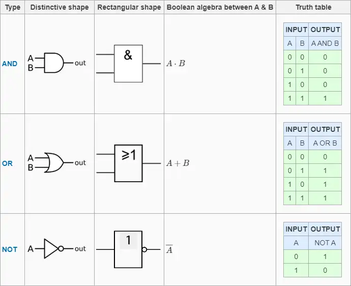
One vital feature : logic gate stays active ,once the input to the logic gate changes, then within a small amount of time, the output will change accordingly.
2. combinational logic
Building up a large network circuits to compute more complex expression needs combine a series of logic gates to generate the same result as the logic function performes.
In this case, there are some restraints on the connection between logic gates:
1. the input of each logic gate <=
(1) system input
(2) the output of other logic gate
(3)the output of the memory elements
2. the system must be acyclic, cannot form inner loop.
3.HCL expression : bit level versus word level as well as membership
HCL expression uses the notion of logic expression in C such as &&, ||, !.
Example : a==b
bool eq = (a&&b)||(!a&&!b); ---- bit level
Example : A==B
bool Eq = (A==B);
Example : Multiplexor
int Out = [
S : A;
1 : B; # default case to end the whole HCL
];
4. bit-level versus word-level combinational circuits
abstract n identical logic model into one model so as to organize all 64 bits into one word as input.
5. ALU
An brief introduction to combinational logic just paves the path for ALU(arithmetic\logic unit), which is a subset of word-level combinational logic.
memory and clocking
A combinational logic discussed before only contains logic gates but no storage device. Clocked registers and random access memory are provided here to control the loading of the input to register and memory and make it appear to a processor that it can access any word within a large address space denoted as virtual address space.
As for register, As long as the clock voltage remines low the state of register won't change. when clock rises, the state of register changes at its input.
1. register file
Each register has two read ports and only one write port, it means that this kind of multiple ports registers allow two read and one write take place simultaneously. There is an appropriate metephor described in the book: register file seems to be a combinational logic but with internal storage. the address is as the inputs and the data is as the output.
2. data memory
The read operation appears to be similar to reading the corresponding value stored in the address at its input as it write signal set to 0; If the address at its input is out of memory the error will be set to 1 because of ADR, and to 0 otherwise.
Writing to memory is controlled by the clock signal with 1 and the error signal arises once there is invalid address and instruction.
4.3 sequential Y86-64 implementation
SEQ is only the first staga for our ultimate goal - an efficient pipelined processor
4.3.1 oragnize processing into stages
several complex concepts introduced here involves one idea : uniformity(minimize complexity). Up to thousand of instructions in Y86-64 are split into a fixed number of stages :
(1) fetch : processor obtains the bytes according to the value of PC where the instruction being executed stores. As the instruction encoding describes, the first byte is separted into high- and low-order 4 bits representated as the icode:ifun and rA:rB respectively. Besides, the updating of PC is accomplised here.
(2) decode : referring the value of register or memory specified in instruction to the CPU
(3) execute : perform arithmetic operation and increment or decrement of %rsp as well as the effective address of memory.
(4) memory : the result is writed to memory
(5) write-it-back : result -> register files
(6) PC update : update PC according to the length of the current instruction
All processes are guranteed as the state of program stay AOK. But if error arises, the program will be halted under the execution of hlt,INS and ADR.
one challenge : how to fit all instructions of Y64-86 within such a framework?
Uniformity! To share as much of hardwares as possible can ease the difficulty for such dizzying set of instructions.
Tracing the detail of each instruction can follow the content from page 423 to 431, especially for instructions pushq and popq.
4.3.2 SEQ hardware structure
designating a structure to satisfies the needs proposed in the last 1 section, the uniformity gives us a clue for structure.
fetch -> decode -> execute -> memory -> wirte it back -> PC update
| stage | description |
|---|---|
| fetch | PC register as address; PC incrementer increases PC |
| decode | read date from register via two ports;memory via one port |
| execute | ALU performs in terms of the arithmetic operation and increment or decrement of %rsp as well as computing the effective address of memory |
| memory | clock && date |
| write it back | register: port E and poer M |
| PC update | vaIP vaIC vaIM |
4.3.3 SEQ timing
A instruction never read back the statae updated by itself in order to complete the instruction.
This principle effectively demonstrates the sequence of push %rsp that the value of push into stack is the decremented value of %rsp.
标签:instruction,--,APP,logic,Y86,part1,64,memory,processor From: https://www.cnblogs.com/UQ-44636346/p/17025965.html